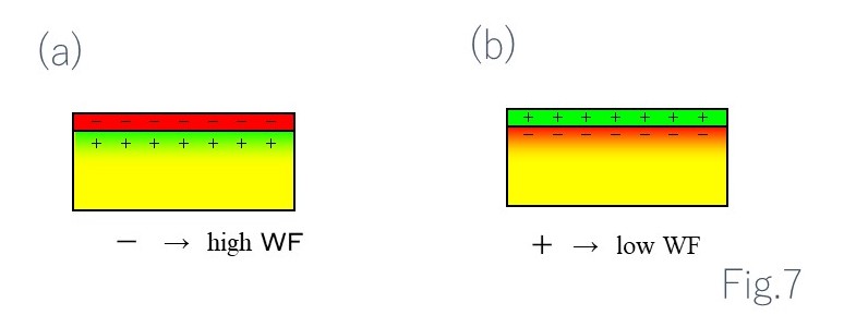
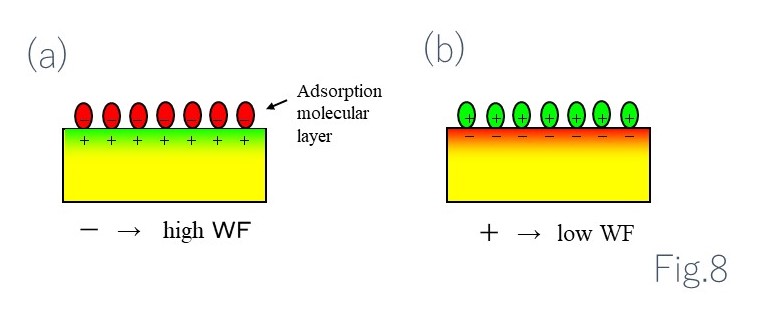
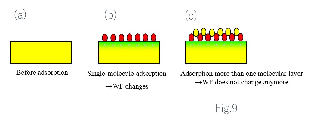
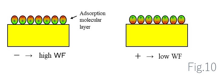
Factors determining work function
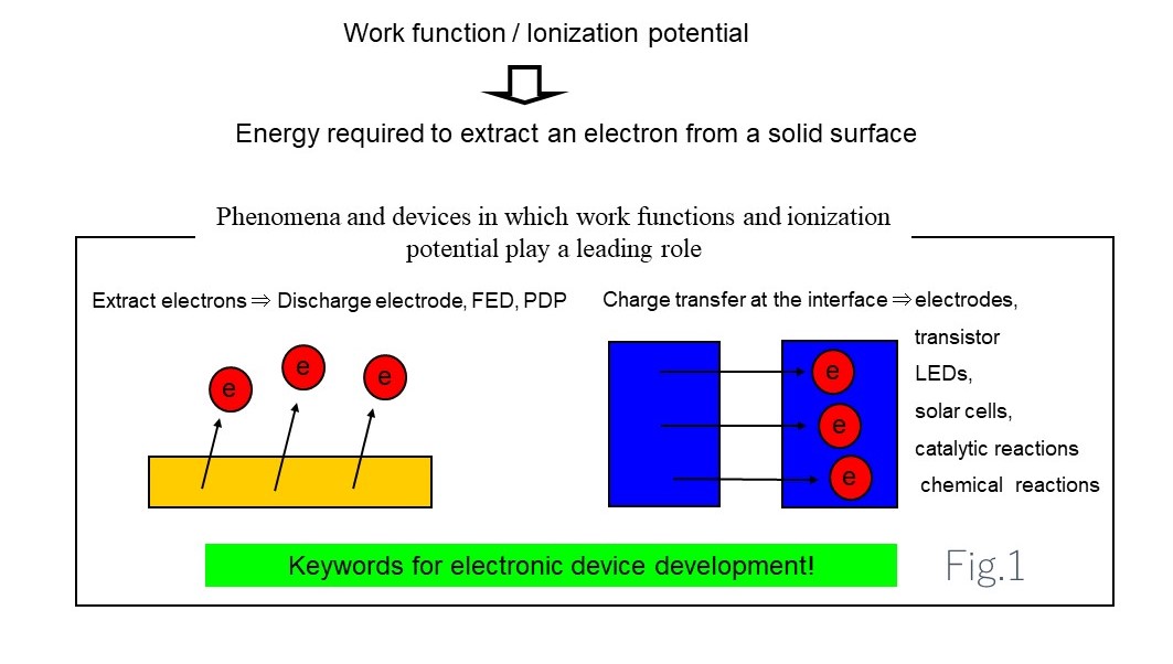
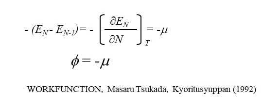
While work function is defined as the minimum energy required to cause an electron excited from the surface of a material, this is expressed as the sum of the bulk property and surface area.
Work function = bulk property + surface area
The bulk property is determined according to the substance. The surface property varies depending on the surface state—i.e. the atomic configuration, structure, and adsorption substances.
Bulk here refers to the solid interior as opposed to the surface.
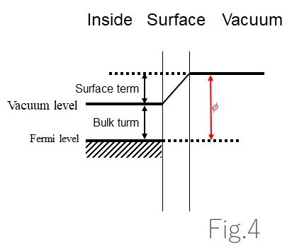
Fig. 4 shows an electronic state diagram for the interior and surface of a metal and the vacuum close to the surface. Exciting Fermi level electrons inside the solid to the vacuum level of the vacuum requires energy with a work function of Φ.
This work function Φ corresponds to the sum of the bulk property (energy difference between the Fermi level and the vacuum level for the interior of a solid with no surfaces) and the surface property (energy difference between the vacuum level of a vacuum subject to surface effects and the vacuum level for the interior of a solid).
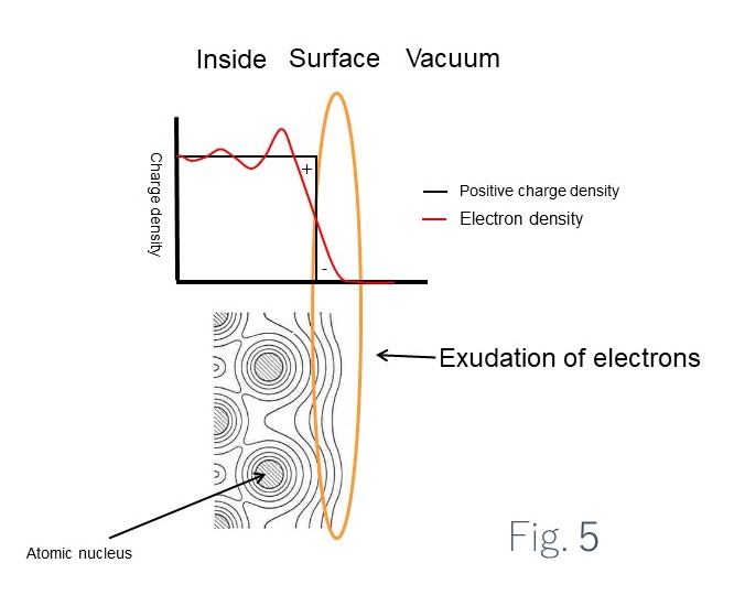
The upper diagram (a) in Fig. 5 shows the electron density inside and at the surface of a metal and in a vacuum close to the surface.
The lower diagram (b) shows the electron density close to atomic nuclei at a metal surface represented as contours.
Within a solid body, the positive charge of the atomic nuclei balances the negative charge of the electrons. A vacuum has no positive charge or electrons. The positive charge is due to the atomic nuclei and is fixed inside the surface. The electrons, however, are able to move, and move toward the vacuum.
The interior of the solid body becomes positively charged based on the movement of the electrons. In other words, the electrons extracted from the interior (when electron moves to the surface compared to when it doesn’t) require excess energy corresponding to the bias toward the positive charge of the solid body interior. This excess energy is the surface property.
The extent of electron movement to a metal surface depends on the orientation of the metal crystals.
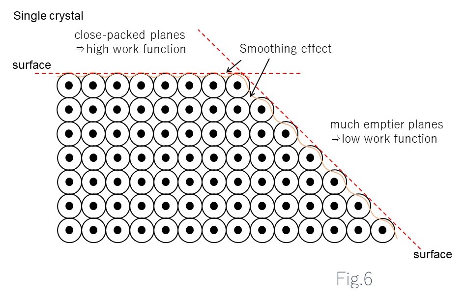
Surfaces at the atomic level are not flat. Rather, they project where atoms are present and are indented where no atoms are present.
Electrons flow from protruding areas to indented areas to make the surface flat.
This is called the flattening effect.
In metal monocrystals in which the atoms are arranged in an orderly pattern, a face may have small gaps between atoms (densely packed face) or large gaps between atoms (less densely packed face), depending on the face when a monocrystal is cut as shown in the figure.
In the case of less densely packed faces with more gaps between atoms, electrons are drawn toward the metal by the flattening effect. On surfaces where the flattening effect is significant, the internal increase in positive charge due to electron movement will be reduced accordingly, resulting in a relatively smaller work function.

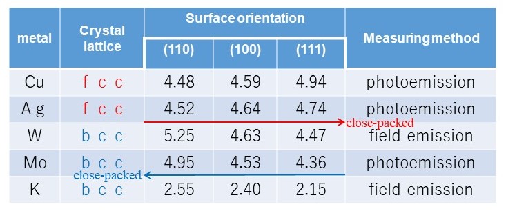
Table.1 work function on a single crystal surface (in vacuum)

This table compares the measured work function for various monocrystal surfaces.
For metals with an fcc crystal lattice, such as Cu or Ag, the atomic density increases for surface orientations in the order 110, 100, 111.
In this case, electron movement to the surface decreases and the work function increases in this order.
For metals with a bcc crystal lattice, such as W, Mo, or K, the atomic density decreases for surface orientations in the order 110, 100, 111.
In this case, electron movement to the surface increases and the work function decreases in this order.
